Thin film deposition is one of the most critical steps in semiconductor manufacturing, where ultra-thin layers of conductive, insulating, and semiconducting materials are deposited onto silicon wafers to build up the complex layered structures of modern integrated circuits. At the heart of these deposition processes-including chemical vapor deposition (CVD), physical vapor deposition (PVD), and epitaxial growth-are graphite susceptors and coated graphite components that hold, heat, and support wafers with exceptional precision and purity. These highly engineered graphite parts are essential to achieving the uniform, defect-free thin films required for advanced semiconductor devices.
Within the global semiconductor graphite market, thin film deposition applications account for 25.6% of total revenue, valued at USD 429.54 million in 2025 according to PW Consulting. This makes deposition the second-largest semiconductor graphite segment after crystal growth, and one of the fastest-growing as chip manufacturers add more deposition layers for advanced 3D device architectures. The market for semiconductor-grade coated graphite components specifically is projected to grow at a 7.8% CAGR through the early 2030s, outpacing overall semiconductor graphite growth as more processes adopt advanced coating technologies to extend component life and improve process performance.
Graphite susceptors function as precision wafer carriers and heating platforms inside deposition chambers. During processing, wafers rest on the susceptor, which is heated either resistively or inductively to precise temperatures ranging from a few hundred degrees Celsius to over 1,000°C depending on the deposition process. The susceptor must heat the wafer uniformly across its entire surface to ensure consistent film thickness and material properties from wafer center to edge. Even temperature variations of just a few degrees can cause unacceptable variations in film thickness, sheet resistance, or material composition, reducing device yield and performance.

Bare graphite is rarely used directly in deposition processes; instead, susceptors and other chamber components are typically coated with a thin layer of silicon carbide (SiC) or other specialized coatings. These coatings serve multiple critical purposes: they prevent particulate generation from graphite substrate erosion, they eliminate carbon contamination of the wafer and deposited films, and they provide a hard, durable surface that withstands repeated wafer loading and unloading cycles. SiC-coated graphite combines the excellent thermal conductivity and light weight of graphite with the extreme hardness, chemical inertness, and purity of silicon carbide, creating a composite component that outperforms alternatives such as pure silicon carbide or quartz.
Beyond susceptors, graphite is used for numerous other deposition chamber components including showerheads for uniform precursor gas distribution, chamber liners, heat shields, electrode assemblies, and focus rings. Each component leverages graphite's unique combination of thermal stability, electrical conductivity, and machinability, typically enhanced with specialized coatings tailored to the specific process chemistry. In epitaxial silicon deposition (EPI) reactors, for example, graphite susceptors with high-purity SiC coatings are the industry standard, enabling precise, uniform growth of single-crystal silicon layers at temperatures above 1,000°C. In PVD sputtering systems, graphite targets and backing plates are used for depositing carbon-based thin films.
The technical requirements for deposition-grade graphite components are extremely demanding. Base graphite material must have exceptional purity with ash content below 5ppm to prevent metallic contamination. It must also have uniform density and thermal conductivity to ensure consistent heating performance across the full wafer diameter. For coated components, the coating must be perfectly uniform, free of pinholes and defects, and have strong adhesion to the graphite substrate to prevent delamination during thermal cycling. And dimensional tolerances are measured in microns, as even slight warping or dimensional change would affect wafer flatness and deposition uniformity.
Huixian Jincheng Abrasive & Graphite Mold Factory, drawing on over 40 years of precision graphite manufacturing experience from its facility in Huixian City, Henan Province, produces high-quality graphite susceptor blanks and uncoated deposition chamber components for the semiconductor equipment supply chain. Founded in 1984, the company has steadily expanded its capabilities to serve the semiconductor industry, building on its core expertise in high-purity graphite processing and precision CNC machining.
Jincheng Graphite manufactures deposition-grade graphite components from premium isostatic graphite materials selected for their uniform density, high thermal conductivity, and low impurity content. The company applies advanced high-temperature purification treatments to reduce ash content to levels suitable for semiconductor processing environments. With over 50 CNC machining centers and maximum processing dimensions of 1,000mm, Jincheng Graphite can fabricate susceptor blanks, chamber liners, showerhead bases, and other deposition components for 200mm and 300mm wafer processing systems, machining complex geometries including pocket features, lift pin holes, and gas distribution channels to tight dimensional tolerances.
The company's multiple vacuum impregnation cycles enhance graphite density and close surface porosity, creating a better substrate for subsequent coating processes and improving the overall quality and durability of finished coated components. Precision surface lapping and polishing achieve extremely flat, smooth surfaces with minimal subsurface damage, which is critical for ensuring uniform coating adhesion and preventing coating defects. Jincheng Graphite works closely with specialized coating partners and semiconductor equipment manufacturers to optimize substrate design and material specifications for specific deposition processes and coating technologies.
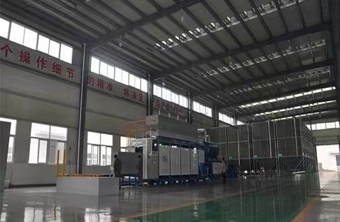
Comprehensive quality control ensures that every graphite component meets the exacting standards required for semiconductor deposition applications. Inspection includes coordinate measuring machine (CMM) dimensional verification, flatness testing, surface roughness measurement, density mapping, and impurity analysis. This rigorous quality assurance gives downstream coating partners and semiconductor manufacturers confidence in the consistency and reliability of Jincheng Graphite's products.
Looking forward, demand for high-performance graphite deposition components will continue to be driven by several powerful industry trends. The ongoing miniaturization of semiconductor devices and the shift to 3D architectures require more deposition steps with tighter uniformity requirements, increasing both the technical demands and value of graphite susceptors and chamber components. The global construction of new semiconductor fabs across all major regions is expanding absolute demand for all types of deposition equipment and their associated graphite consumables. And advancing coating technologies including next-generation SiC formulations and new ceramic materials are extending component service life while enabling more aggressive process conditions.

For graphite manufacturers like Jincheng Graphite, the deposition equipment supply chain represents a high-value, technology-driven market segment with strong growth fundamentals. While full coated component production requires specialized coating capabilities, high-quality graphite substrate manufacturing is itself a technically demanding and valuable niche. As China's semiconductor equipment industry continues to advance and domesticate its supply chain, domestic graphite specialists like Jincheng Graphite with the precision and purity capabilities to serve deposition applications are well-positioned to capture growing market share in this critical high-tech sector.